Semiconductors » P-n junction
P-N Semiconductor
P-N semiconductor is the combination of both p-type semiconductor and n-type semiconductor to utilize the properties of both semiconductors. It is formed when a p-type semiconductor and an n-type semiconductor are joined together without disturbing their properties.
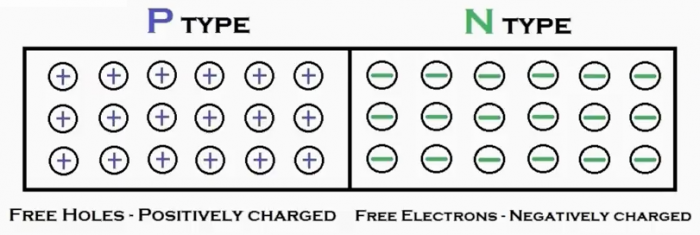
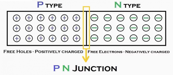
Image source:techtechtrix.com
The region, which connects p-type and n-type semiconductors, is called P-N Junction.
When a P-N junction is made, electrons and holes near the junction get attracted to each other and moves from one region to another. This movement of electrons and holes across the p-n junction creates a region called “depletion region” or “space charge region” or "depletion layer"
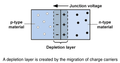
Image source: TechnologyUK.net
In the ‘depletion region’, electrons migrate from n-type to p-type and become positively charged, and holes migrate from p-type to n-type and become negatively charged. This will cause a POTENTIAL BARRIER or JUNCTION BARRIER built up at the junction. Built up of potential barrier stops further migration of holes and electrons and become equilibrium. The barrier potential is approximately 0.2V for Germanium and 0.6V for Silicon. The migration takes place until it reaches equilibrium. Continuous movement of holes and electrons in the ‘space charge region’ induces electricity. This electric current is called diffusion current.
Reverse biased
If the voltage is negative in an ideal diode the current will not pass through. The diode would act like an open circuit and said to be off or reverse biased. When an external dc supply is connected to the diode with negative terminal (-ve) to p-type region and positive terminal (+ve) to n-type region, the depletion region widens (increases potential barrier) and no current will flow through the circuit. This circuit is called reversed biased.
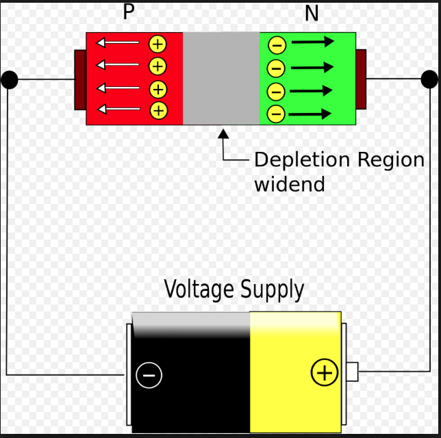
Image source: wikibooks.org
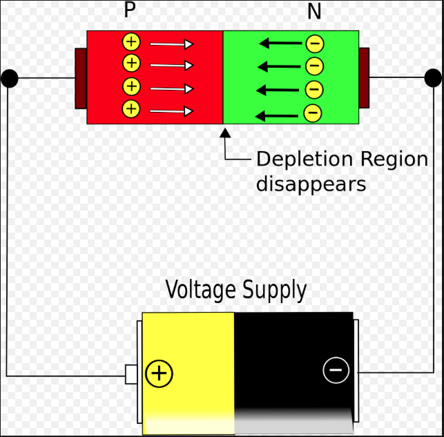
Forward biased
As long as the voltage across the diode is not negative the diode would conduct current. Ideally a diode would “turn on” and act like a short circuit and conduct current even at zero voltage. When a diode is conducting current its said to be a forward biased. When an external dc supply is connected to the diode with negative terminal (-ve) to n-type region and positive terminal (+ve) to p-type region, the depletion region narrows (decreases potential barrier) and the current will flow through the circuit. This circuit is called forward biased.
A device that allows current only in one direction is called a diode, thus p-n junction is a diode.